Special ceramics such as zirconia and alumina ceramics have good wear resistance, high temperature resistance and corrosion resistance. Therefore, they are more and more applied to industrial components.
3.Rough machining: uses surface grinding, internal and external grinding, centerless grinding to finish the surface finish, and polishing machine to process other internal or curved surface finish.
Machining Ceramic Part ,Customized Machining Ceramic Part ,Ceramic Blade,Advanced Ceramic Dongguan Mingrui Ceramic Technology Co.,Ltd , http://www.mr-ceramics.com
"I know there is a problem with my design, but I didn't find the internal visibility needed for the problem quickly." Debugging an FPGA-based system can be frustrating due to a lack of sufficient internal visibility. With the use of larger FPGAs that typically include the entire system, the ability to visualize debugging becomes a big problem. To gain internal visibility, design engineers must use some pins exclusively as debug pins instead of actually designing them. Which tools are available for internal FPGA trace measurements? What other technologies can use a fixed number of pins to maximize internal visibility?
FPGA design engineers have two methods for performing internal trace measurements:
1. Route the node to the pin and test using a traditional external logic analyzer.
2. Insert a logic analyzer core into the FPGA design and route the traces stored by the internal FPGA memory through JTAG.
Logic Analysis FPGA developers must make important decisions early in the design process. They consciously or unconsciously determine how they can debug their designs. The most common way to get internal FPGA visibility is to use a logic analyzer that routes the internal nodes of interest to the pins probed by the analyzer. This method provides deep memory traces where the cause of the problem and its effects can be very large. Logic analyzers are good at measuring asynchronous events that may escape simulations. One example is the interaction of two or more clock domains with non-relevant frequencies. Logic analyzers provide powerful triggers and the resulting measurements can be correlated with the timing of other system events.
Traditional logic analyzers provide status and timing modes so data can be captured synchronously or asynchronously. In timing mode, design engineers can see the relationship between signal transitions. In the state mode, the design engineer has the ability to observe the bus relative to the state clock. State mode is particularly useful when debugging bus-critical data paths.
Effective real-world measurements require careful planning. The main trade-off to consider with traditional logic analyzers is to route the nodes to detectable pins. Traditional logic analyzers can only observe signals routed to pins. Since potential in-circuit debugging problems are not yet known, design engineers can only use very few pins for debugging. Such a small number of pins may not be enough to provide enough visibility to solve the problem at hand, delaying the completion of the project.
One way to maintain internal visibility while reducing the number of pins dedicated to debugging is to insert a switch multiplexer in the design (see Figure 1). For example, when the FPGA design enters the circuit, it may need to observe 128 internal nodes, which requires tracking 32 channels at a time. In this case, a multiplexer can be implemented in the FPGA design to route 32 nodes at a given time. To program a multiplexer, the design engineer can download a new configuration file and switch the signals via JTAG or via a control line on the multiplexer. During the design phase, the test multiplexer insertion must be carefully planned. Otherwise, the design engineer may stop at the same time to access the node that needs to be debugged.
Figure 1: The insertion of the test multiplexer allows the design engineer to route a subset of the internal signals. The traces captured by the Agilent 16702B are shown. 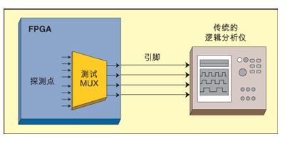
The second method of minimizing the number of debug dedicated pins is time division multiplexing (TDM). TDM multiplexing is often used for design prototypes, where multiple FPGAs are used as prototypes for a monolithic ASIC to minimize the number of dedicated debug pins. This technique is best suited for handling slower internal circuits. Assume that a 50-MHz design using an 8-bit bus (20 ns between clock edges) requires in-circuit visibility. Use 100MHz to sample the low 4bit during the first 10ns and sample the high 4bit during the second 10ns. This will use only 4 pins to capture all 8 bits of debug information every 20ns cycle. After capturing the trace, the 8-bit trace can be reconstructed by combining successive 4-bit captures. TDM multiplexing also has some drawbacks. If you use traditional logic analyzers to capture traces, triggering becomes very complicated and error-prone. For example, triggering on 8-bit patterns includes setting the logic analyzer to look for another specific 4-bit pattern following the specified 4-bit pattern. However, the logic analyzer does not know which of the 4 bits is the beginning of the 8-bit group and therefore triggers on the conditions that match the trigger settings - not the user-intended trigger conditions.
The measurement results obtained using TDM multiplexing have precise cycles. However, the design engineer lost the timing relationship information during the clock cycle. The speed of the single-ended pin and the acquisition speed (status mode) of the logic analyzer collection trace limit the compression ratio. For example, if the maximum single-ended pin speed is 200 MHz and the internal circuit operates at up to 100 MHz, the maximum compression ratio that can be achieved is 2:1.
As a given FPGA design matures, it may be enhanced and changed. The original pins that are dedicated to debugging will be used for design enhancements. Or start to limit the design of the pin. Another debugging technique brings value to such situations.
Logical Analysis Cores Most FPGA vendors now provide logic analysis (see Figure 2). These IPs are inserted into the FPGA before or after synthesis. The core contains flip-flop circuitry and resources for setting up measurements and internal RAM to hold traces. Inserting the logic of the design analysis core changes the timing of the design, so most design engineers leave the kernel permanently in the design. 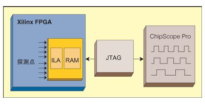
The example in the figure is Xilinx ChipScope Pro.
For in-circuit configuration, the kernel can be accessed via JTAG and captured data can be transmitted to the PC for observation. If the core consumes less than 5% of the available resources, the FPGA core is fully functional. If the size of the FPGA causes the kernel to consume more than 10% of resources, design engineers will encounter many problems when using this method.
The logic analysis kernel has three main advantages.
1. Their use does not increase the pin. It can be accessed via dedicated JTAG pins already on the FPGA. This debugging method can also gain internal visibility even if no other pins are available.
2. Simple detection. Probes include inputs that route the nodes to the internal logic analyzer. There is no need to worry about how to connect to a circuit board for effective information and there are no signal integrity issues.
3. Logical Analysis The kernel is cheap. FPGA vendors base their business models on the value gained from silicon. Therefore, the debug IP used can usually be obtained at a price lower than $1,000.
The use of internal logic to analyze the kernel also has three effects.
1. The size of the kernel limits its use in large FPGAs. In addition, because the internal FPGA memory is used for the trace, the trace depth is very shallow.
2. The design engineer must give up the internal memory for debugging and the memory will be used by the design he has made.
3. The internal logic analyzer only works in state mode. The data they capture is synchronized with the specified clock and cannot provide a signal timing relationship.
Hybrid Technologies Some FPGA vendors have begun to develop combined technologies with traditional logic analyzer vendors (see Figure 3). For example, Agilent and Xilinx recently jointly developed 2M deep memory for Xilinx's ChipScope.
Figure 3: The first example of mixed internal and conventional logic analysis is the deep memory developed by Agilent and Xilinx in conjunction with ChipScope Pro. The number of pins can be minimized through TDM multiplexing.
This solution uses the internal logic analysis kernel for triggering. When the core trigger condition is satisfied, the core transfers trace information from the routed node to the core and then to the pin. The pin is connected to a small external tracking box via the mictor connector. This solution incorporates TDM multiplexing to reduce the number of debug dedicated pins. Depending on the speed of the internal circuit, multiplexing compression may be 1:1, 2:1, or 4:1. Since the trace is not stored internally, the IP core is smaller than the logical analysis IP with trace memory.
How to make a decision?
Traditional logic analysis and kernel-based logic analysis techniques are useful. When choosing the solution that best suits your debugging needs, considering some factors in advance will help you make the decision. The following questions can help you determine which plan is most effective.
1. What type of debugging problems do you expect to encounter? Internal logic analyzers can find simpler problems, while traditional logic analyzers can handle complex faults.
2. In addition to the status mode, do you still need to capture timing information? If needed, traditional logic analyzers can adapt to this requirement.
3. How deep is the trace? Traditional logic analyzers can capture up to 64M traces on each channel, while internal logic analysis cores are more suitable for shallow traces.
4. How many pins can be dedicated to debugging? The smaller the pin count, the more suitable it is to use an internal logic analyzer.
5. How much money must be invested for new tools? Although the 32-channel traditional logic analyzer starts at $6K, the internal logic analyzer and accompanying waveform viewers start at less than $1K.
6. Can the development team tolerate the impact of FPGA design? The kernel can only work on large FPGAs and will change the timing of the design. For all sizes and types of FPGAs, the routing signal output of traditional logic analyzers has little impact on design and operation.
share to:
(This article is taken from the world of electronic engineering: http://Test_and_measurement/2008/0523/article_161.html)
Ceramic components can be customized for various shapes, with different processing techniques for different shapes.
1.Pore processing: the main method is using honing machines, CNC engraving and milling machine, Internal and external grinder and other advanced processing equipments.ceramic products can be cutting, carving and punch.The accuracy of the pore can meet the requirements at a very high precision.
2.Plane machining:There are a lot of methods to process the plane of ceramics, almost all the basic processing methods can be used to process the plane.such as car, milling, planing, grinding, drawing, wire cutting.The most widely used method is surface grinder

FPGA in-circuit debugging based on logic analysis kernel
As FPGAs become more and more capable, the need for effective debugging tools will become crucial. The careful planning of internal visibility will enable the development team to adopt the correct debugging strategies to complete their design tasks faster. Figure 2: Logic analyzer configuration downloaded from JTAG,